


Products Description
Features
l Operating Data Rate up to 4.25Gbps
l Single 3.3V Power Supply and CML Logic Interface
l 850nm VESCL transmitter and high performance PIN receiver
l Link Distance up to 300m with 50/125µm multi-mode fiber
l Low EMI and excellent ESD protection
l Built-in Digital Diagnostic Monitoring (DDM) function,Compliant with SFF-8472
l Operating Case Temperature
Standard(C): 0℃~+70℃
l Industrial(I): -40℃~+85℃
Applications
l 1.063/2.125/4.25Gbps Fiber Channel
l Other optical Links
General
The GIGAC's GACS-8548-02x series is a multi-rate 850nm SFP which ensures compliance to 4.25Gbps Fibre Channel specifications without the need for Rate Select. mode transceiver is small form factor pluggable module for serial optical data communications such as IEEE 802.3ae . It is with the SFP 20-pin connector to allow hot plug capability. This module is designed for multi-mode fiber and operates at a nominal wavelength of 850nm. The transmitter section uses a 850nm VCSEL laser and is a class 1 laser compliant according to International Safety Standard IEC-60825.
Order Information
Table 1-Order Information
Part Number | Data Rate | Wavelength | Distance | FiberNote2 | Interface | Temp.Note1 |
GACS-8548-02 | 4.25Gbps | 850nm | 300m | MMF | Duplex LC | 0℃~+70℃ |
GACS-8548-02I | 4.25Gbps | 850nm | 300m | MMF | Duplex LC | -40℃~+85℃ |
Note: 1. Case Temperature
Note: 2. “MMF” stands for 50/125µm MMF
Absolute Maximum Ratings
Table 2-Absolute Maximum Ratings
Parameter | Condition | Unit | Min. | Typ. | Max. |
Supply Voltage | +3.3v Supply Voltage | V | -0.5 | - | 3.6 |
Storage Temperature | Case Temperature | ℃ | -15 | - | 90 |
Relative Humidity, Storage | None Condensing | % | 5 | - | 95 |
*Exceeding any one of these values may destroy the device immediately.
Operating Environment
Table 3-Operating Environment
Parameter | Condition | Unit | Min. | Typ. | Max. |
Power Supply Voltage | +3.3v Supply Voltage | V | 3.13 | 3.3 | 3.47 |
Power Dissipation | W | - | - | 1.5 | |
Operating Case Temperature | Standard | ℃ | 0 | - | 70 |
Industrial | ℃ | -40 | - | 85 | |
Gbps | - | 4.25 | - |
Electrical Characteristics
Table 4-Electrical Characteristics
Parameter | Symbol | Min | Type | Max | Units | Notes | |
Transmitter | |||||||
Differential Data Input Swing | Vin | 400 | - | 1200 | mVpp | 1 | |
Input Differential Impedance | Zin | 90 | 100 | 110 | ohm | ||
Tx_Disable | Disable | VD | 2.0 | - | VCC | V | |
Enable | VEN | GND | - | GND+0.8 | V | ||
TX_ Fault | Fault | VF | 2.0 | - | VCC | V | |
Normal | VNO | 0 | - | +0.8 | V | ||
Receiver | |||||||
Differential Date Output Swing | Vout | 300 | - | 950 | mVpp | 2 | |
Output Differential Impedance | Zout | 90 | 100 | 110 | ohm | ||
Rx_Los | Los Signal | VOH | 2.0 | - | VCC+0.3 | V | |
Normal Operation | VOL | GND | - | GND+0.8 | V | ||
Note:
1. Internally AC coupled, input termination may be required for CML applications.
2. Internally AC coupled, CML differential output stage.
Optical Characteristics
Table 5-GACS-8548-02/GACS-8548-02I, SFP 4.25G 300m
Parameter | Symbol | Unit | Min | Type | Max | Notes |
Distance | L | m | - | - | 300 | |
Bit Rate | BR | Gbps | - | 4.25 | - | |
Optical transmitter Characteristics | ||||||
Center Wavelength Range | λc | nm | 800 | 850 | 900 | |
Average Launch power Tx_off | Poff | dBm | - | - | -30 | |
Spectral Width (RMS) | Δλ | nm | - | - | 0.6 | |
Launch Optical Power | PO | dBm | -9 | - | -1 | 1 |
Extinction Ratio | ER | dB | 3.5 | - | - | |
Eye Diagram | Compliant with IEEE 802.3-2005 | |||||
Optical Receiver Characteristics | ||||||
Receiver Sensitivity | Sens | dBm | - | - | -15 | 2 |
Saturated optical power | PSAT | dBm | -1 | - | - | |
Center Wavelength Range | λc | nm | 800 | 850 | 900 | |
LOS | LOSD | dBm | - | - | -16 | |
LOSA | dBm | -35 | - | - | ||
LOS Hysteresis | dB | 0.5 | - | - | 3 | |
Note 1.Coupled into 50/125 MMF.
Note 2.Measured with PRBS 2^31-1 test pattern @4.25Gbps.BER=10E-12
Note 3.LOS Hysteresis, See Figure1
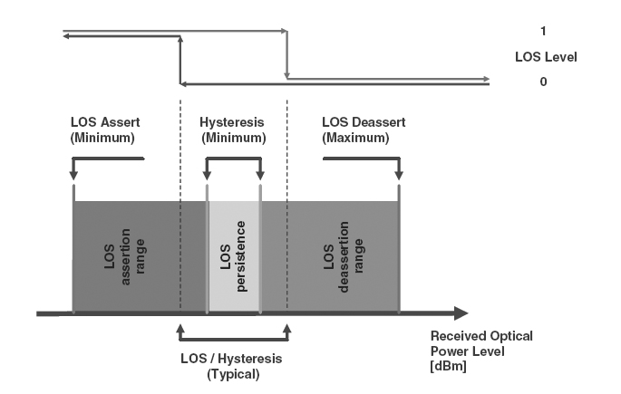
Figure 1 LOS Hysteresis
Recommended Host Board Power Supply Circuit
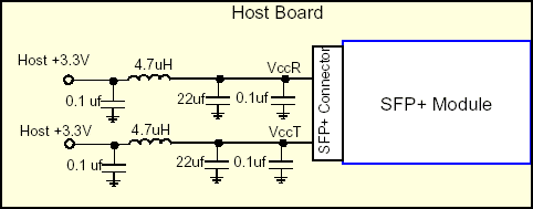
Figure 2 Recommended Host Board Power Supply Circuit
Recommended Interface Circuit
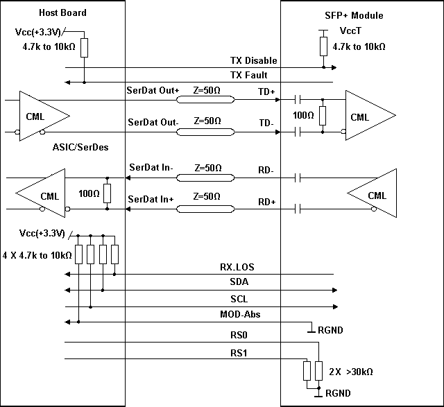
Figure 3 Recommended Interface Circuit
Pin arrangement
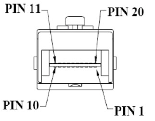
Figure 4 Pin arrangement
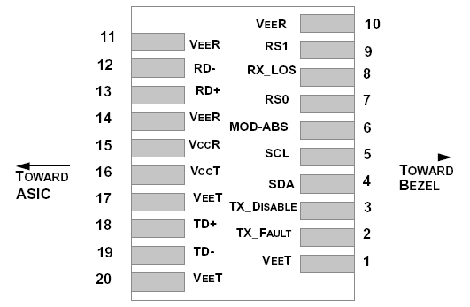
Figure 5 Pin View
Table 6-Connector Pin Assignment
Pin | Name | Function | Notes |
1 | VEET | Transmitter Ground | |
2 | TX_FAULT | Transmitter Fault Indication | Note 1 |
3 | TX_DISABLE | Transmitter Disable | Note 2 |
4 | SDA | Module Definition 2 | Note 3 |
5 | SCL | Module Definition 1 | Note 3 |
6 | MOD-ABS | Module Definition 0 | Note 3 |
7 | RS0 | Not Connected | |
8 | Rx_LOS | Loss of Signal | Note 4 |
9 | RS1 | Not Connected | |
10 | VEER | Receiver Ground | |
11 | VEER | Receiver Ground | |
12 | RD- | Inv. Received Data Out | Note 5 |
13 | RD+ | Received Data Out | Note 5 |
14 | VEER | Receiver Ground | |
15 | VccR | Receiver Power | 3.3 ± 5% |
16 | VccT | Transmitter Power | 3.3 ± 5% |
17 | VEET | Transmitter Ground | |
18 | TD+ | Transmit Data In | Note 6 |
19 | TD- | Inv. Transmit Data In | Note 6 |
20 | VEET | Transmitter Ground |
Note:
1.TX Fault is open collector output which should be pulled up externally with a 4.7K ~10KΩ resistor on the host board to voltage between 2.0V and VCC+0.3V. Logic 0 indicates normal operation; logic 1 indicates a laser fault of some kind. In the low state, the output will be pulled to less than 0.8V.
2.TX Disable input is used to shut down the laser output per the state table below. It is pulled up within the module with a 4.7~ 10K resistor.
Low (0- 0.8V): Transmitter on
Between (0.8V and 2V): Undefined
High (2.0 – VccT): Transmitter Disabled
3.MOD-DEF 0, 1, 2. These are the module definition pins. They should be pulled up with a 4.7~10K resistor on the host board to supply less than VccT+0.3V or VccR+0.3V.
MOD-DEF 0 is grounded by the module to indicate that the module is present.
MOD-DEF 1 is clock line of two wire serial interface for optional serial ID.
MOD-DEF 2 is data line of two wire serial interface for optional serial ID.
4.LOS (Loss of signal) is an open collector output, which should be pulled up with a 4.7k~10kΩ resistor on the host board to a voltage between 2.0V and Vcc+0.3V. Logic 0 indicates normal operation; logic 1 indicates loss of signal. In the low state, the output will be pulled to less than 0.8V.
5.These are the differential receiver outputs. They are AC-coupled 100Ω differential lines which should be terminated with 100Ω differential at the user SERDES. The AC coupling is done inside the module and thus not required on the host board.
6.These are the differential transmitter inputs. They are AC-coupled, differential lines with 100Ω differential termination inside the module.
Digital Diagnostic Memory Map
The SFP series defines a 256-byte memory map in EEPROM describing the transceiver’s capabilities, standard interfaces, manufacturer, and other information, which is accessible over a 2 wire serial interface at the 8-bit address 1010000X (A0h),see Figure. The memory contents refer to SFF-8472 Rev 9.5. A2 EEPROM Definition Specific settings please consult our engineer.
Figure 6 Memory Map
Mechanical Information
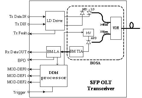
Figure 7 LC interface package
Regulatory Information
Table 7-List of Regulatory Compliance
Feature | Standard | Performance |
Electrostatic Discharge (ESD) to the Electrical Pins | MIL-STD-883H Method 3015.8 | Based on HBM |
IEC61000-4-2 | 8kV Contact Discharge 15kV Air Discharge | |
Electrostatic Discharge to the enclosure | EN 55024:1998+A1+A2 IEC-61000-4-2 GR-1089-CORE | Compatible with standards |
Electromagnetic Interference (EMI) | FCC Part 15 Class B EN55022:2006 CISPR 22B :2006 VCCI Class B | Compatible with standards Noise frequency range: 30MHz to 6GHz. Good system EMI design practice required to achieve Class B margins. System margins are dependent on customer host board and chassis design. |
Immunity | EN 55024:1998+A1+A2 IEC 61000-4-3 | Compatible with standards. 1KHz sine-wave, 80% AM, from 80MHz to 1GHz. No effect on transmitter/receiver performance is detectable between these limits. |
Laser Eye Safety | FDA 21CFR 1040.10 and 1040.11 EN (IEC) 60825-1:2007 EN (IEC) 60825-2:2004+A1 | CDRH compliant and Class I laser product. |
RoHS2.0 | 2011/65/EU | Compliant with standards |
Notice
Gigac reserves the right to make changes to or discontinue any optical link product or service identified in this publication, without notice, in order to improve design and/or performance. Applications that are described herein for any of the optical link products are for illustrative purposes only. Gigac makes no representation or warranty that such applications will be suitable for the specified use without further testing or modification.
Revision History
Version | Initiated | Reviewed | Revision History | Release Date |
A0 | Eli.Huang | Sean.Lin | Initialization | 2020-06-20 |
A1 | Eli.Huang | Sean.Lin | Partial parameter update | 2023-03-07 |
Contact
Add: Area 3-502, Haolang technology Park,
NO.2666, Konggang Four Road, Shuangliu district, 610207 Chengdu, China
Tel: (+86) 028-85124518
Fax: (+86) 028-85154518
Postal: 610207
E-mail: sales@gigac.com
Website: http://www.gigac.com
Our factory
 and combiner unit (OMU)")
Wavelength Divisio···

Detailed Explanati···

The Working Princi···

The Key Difference···
Hot Tags:
R&D laboratory
Gigac has introduced numerous precision testing equipment, such as Ixia XGS12, Ixia WaveTest 93, Anritsu, Fujikura, Fluke, JDSU, Agilent, EXFO, DATA-PIXEL, etc., for product development testing and validation.At present, there are over 100 professional engineers, of which 50% are senior engineers. Through standardized testing processes and in line with international professional testing standards, we provide testing in various aspects such as product appearance, performance, compatibility, and solution scenarios to meet the diverse testing needs of global customers.
Numerous research and development achievements
Gigac adopts a research and development model that combines independent research and joint development, and has achieved outstanding results in industrial design and product software and hardware research and development.As data centers continue to expand and grow, a well planned cabling infrastructure is crucial. Without flexible cabling plans that can easily adapt to common moves, additions, and changes, your network growth will be limited. The Gigac series high-density data center cabling solutions can simplify deployment, enabling up to 144 LC fibers in 1U, and enabling flexible expansion and rapid upgrades with increasing business traffic demands.
Gigac Test Center
Gain a comprehensive understanding of Gigac's optical modules, fiber optic jumpers, and enterprise network testing center. We have a comprehensive testing plan, professional testing equipment, and standard testing procedures. We regularly test optical modules, cables, switches, and other products to ensure that we provide high-quality products to our partners.
