

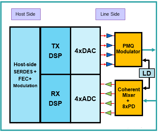
Figure 1. Functional diagram of coherent optical module (single disk)
As shown in the above figure, in the coherent optical module, at the transmitting end, the customer's electrical signal is processed by the digital signal processing function in the DSP chip to complete the symbol of specific probability distribution and QAM mapping, including probability distribution matching, FEC coding, QAM mapping and other functions. Then, the baseband digital QAM signal is subjected to signal spectrum shaping and pre compensation at the transmitting end to compensate for the imperfect characteristics of the optoelectronic device. After processing by these DSPs, it is sent to a four channel high-speed DAC and converted into a high-speed analog bandwidth electrical signal through digital to analog conversion. After being amplified by the driver, it is loaded onto a polarization multiplexed optical IQ modulator to complete up conversion. The base charged signal is loaded onto the amplitude, phase, and two orthogonal polarization states of the optical carrier. After being controlled by the optical amplifier/attenuator inside the optical module for optical power, it is output to generate a high-speed optical signal.
At the receiving end, the high-speed optical signal undergoes coherent mixing and photoelectric conversion under the action of local oscillator light after passing through ICR to obtain the baseband electrical signal. Then, it is sampled by high-speed ADC to achieve digitalization of the electrical signal. With the powerful DSP equalization ability of the receiving end, the signal is compensated for the damage it experiences in the circuit and optical transceiver module. The processing flow of the receiving DSP sequentially includes resampling, optical front-end compensation, dispersion compensation, clock recovery, polarization demultiplexing adaptive equalization, frequency offset estimation, phase recovery, constellation mapping, and FEC decoding. Linear IQ modulation and coherent detection of the optical field enable the receiving end to theoretically recover all the optical field information of the optical signal. DSP processing can perfectly compensate for the linear damage experienced by the optical signal, such as inter channel skew, IQ amplitude and phase imbalance, fiber chromatic dispersion (CD) and polarization mode dispersion (PMD), frequency offset and phase noise, etc. Even through special algorithm design, the nonlinear effects of the system can be compensated or balanced to a certain extent. For example, digital subcarrier multiplexing can enhance the tolerance for fiber nonlinearity. The high-performance SD-FEC algorithm in 800G coherent DSP chips has better error correction ability compared to HD-FEC in early 100G DSP chips, further improving the OSNR tolerance of signals and ensuring error free transmission in suitable application scenarios.
Furthermore, on the internal or external single disk of the optical module, the connection between the line side electrical signal and the customer side electrical signal can be achieved through Gearbox or Framer chips, completing different functions such as forwarding and multiplexing. Of course, other auxiliary chips are also needed in the optical module, such as power chips, clock chips, FPGA control chips, and temperature monitoring chips. In addition, the DSP chip should also have SerDes function to better interconnect with customer side signals.
In general, the core chips in coherent optical modules can be divided into two categories: optical chips, including bipolar IQ modulation, lasers, coherent optical mixers, and balanced detectors; Electric chips, including modulator drivers, transimpedance amplifiers (TIAs), and DSP chips. From the perspective of chip manufacturing technology, current electric drives are based on Si or SiGe materials using CMOS standard process flow. Due to power consumption and performance requirements, the core DSP chip needs to adopt a relatively advanced 7nm node process.
Table 1. Performance comparison of different devices made from different materials
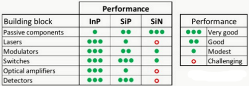
And optical chips can be divided into two categories, one is based on III-V group materials such as InP, including lasers, modulators, and detectors (GaAs). The second is based on Si basis, including Si based modulators, coherent receivers, etc. Although in recent years, with the increasing requirements for device integration and co packaging, SiP has become a hot topic in academia and a new favorite in the industry, fundamentally speaking, there is no consensus on who is good or bad for InP versus SiP for coherent optical modules. Overall, both have their strengths, as shown in Table 1.
The InP platform is better at making active devices, while SiP performs better on passive devices. SiP has advantages in production and cost, but may not be as good as InP in bandwidth and performance. The InP platform can integrate/package lasers with CDM and ICR, while SiP can integrate/co package DSP and PIC without lasers. SiP has many advantages, but its undeniable drawbacks include two: firstly, it has high coupling loss with optical fibers, and secondly, it cannot emit light itself (the LED distance practical optical communication application developed by Dr. MIT is still early). Rather than saying who replaces who, it may be necessary to consider how to combine the advantages of both, such as Si+X, hybrid integration, to optimize both cost and performance as much as possible.
