


Products Description
Product Features
Complies with the requirements of CPCI bus usage, can replace ordinary leaf spring 2mm pitch connectors,
With reliable contact performance and environmental resistance
Electrical and environmental performance complies with IEC61076-4-101
Uses highly reliable hyperbolic wire spring holes, suitable for harsh environments with strong vibration and shock
Suitable for high-speed data transmission between motherboard and daughterboard
Excellent signal integrity
Transmission rate can reach 3.125Gbps
Can be used in military fields such as aviation, aerospace, and naval ships
Mechanical properties
• Mechanical life: 5,000 cycles of insertion and extraction
• Shock: 6ms post-peak sawtooth wave, 980m/s²
• Vibration: Sine wave from 10Hz to 2000Hz, acceleration of 196m/s²;
Random vibration from 10Hz to 2000Hz, power spectral density of 0.4g²/Hz
Electrical properties
• Voltage withstand: 1000V AC at normal temperature and pressure;
100V AC at low pressure (30KPa)
• Contact resistance: ≤25mΩ
• Insulation resistance: ≥5000MΩ
• Rated current: 1A

Environmental Performance
• Operating Temperature: -65℃ to +125℃
• Fluid Resistance: Resistant to various fuels, coolants, and solvents
• Damp Heat: As per GJB 1217A, alternating damp heat for 10 days
• Flame Retardancy: Self-extinguishes within 10 seconds
• Salt Spray: 48 hours
Utilizes spring-loaded pin holes to enhance contact reliability
The K2 series connectors employ highly reliable wire spring sockets, capable of withstanding harsh operating conditions such as high-intensity vibrations and shocks. Their resistance to vibration and shock is significantly higher than that of ordinary leaf spring structure products. Additionally, their mechanical life exceeds 5000 cycles, far surpassing the 500 cycles of ordinary leaf spring structure products.
Performance Comparison
Category | Ordinary Leaf Spring Structure | K2 Series |
Mechanical Life | 500次 | 5000次 |
Vibration Resistance | 10Hz~2000Hz,196m/s2 | 10Hz~2000Hz,0.4G2/Hz |
Shock Resistance | 490m/s2 | 980m/s2 |
Reversed pin hole installation enhances operational reliability.
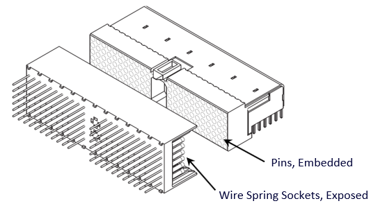
The K2 series connector sockets (backplane connectors) adopt an exposed socket structure, while the plugs (daughterboard connectors) utilize an embedded pin structure. This design enhances the structural strength of the exposed parts, preventing issues such as pin bending and breakage caused by accidental knocks during insertion and separation, which are common problems with ordinary leaf spring connectors due to their exposed pins and lower strength.
Installation Comparison of K2 Series and Ordinary Leaf Spring Structure Sockets
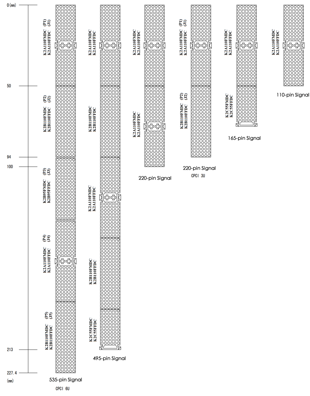
Rows a to e are signal contacts, while rows f and g are shielding contacts. When the signal contacts of the K2 series connector overlap with those of an ordinary leaf spring structure connector, due to the structural differences between the two types of connectors, there will be a 1mm deviation in the outer walls of the two connectors. The specific relative positions are shown in the figure below.
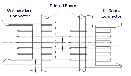
The relative position dimensions between the printed board, motherboard, and connector

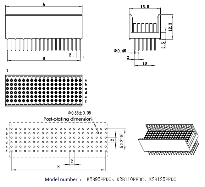
Product outline dimensions and printed board package size
Type A plug of K2 series

Type A socket of K2 series

Type B plug of K2 series
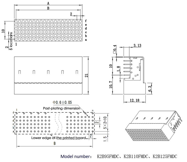
Number of cores | 95 cores | 110 cores | 125 cores |
A | 37.98 | 43.98 | 49.98 |
B | 36 | 42 | 48 |
n | 19 | 22 | 25 |
Type B socket of K2 series
Number of cores | 95 cores | 110 cores | 125 cores |
A | 37.98 | 43.98 | 49.98 |
B | 36 | 42 | 48 |
n | 19 | 22 | 25 |
Example of Connector Combinations
The K2 series connectors are designed for CPCI bus systems, serving as a replacement for conventional leaf spring connectors with a 2mm pitch. In practical applications, to prevent lateral and angular errors, it is common to pair Type B connectors, which do not have error-proofing devices, with Type A connectors that do have such devices. The extended assembly (Type C) should only be used at the end of the connector chain and must be paired with at least one Type A connector featuring error-proofing devices. Below are several commonly used combination methods.
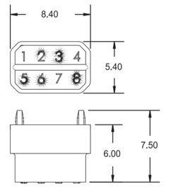
Error-Proofing or Mis-Insertion Prevention Device
The coding pieces can be installed into the Type A connectors of the K2 series. They need to be ordered separately.
Coding pieces for module ends

coding pieces for backplane ends.
Module End Coding Piece | Backplane End Coding Piece | |||
Coding | Ordering Model | Coding | Ordering Model | |
1234 | K2KM1234 | 5678 | K2KF5678 | |
1256 | K2KM1256 | 3478 | K2KF3478 | |
1258 | K2KM1258 | 3467 | K2KF3467 | |
2348 | K2KM2348 | 1567 | K2KF1567 | |
2358 | K2KM2358 | 1467 | K2KF1467 | |
2478 | K2KM2478 | 1356 | K2KF1356 | |
2567 | K2KM2567 | 1348 | K2KF1348 | |
3567 | K2KM3567 | 1248 | K2KF1248 | |
4578 | K2KM4578 | 1236 | K2KF1236 | |
6321 | K2KM6321 | 8754 | K2KF8754 | |
印制板布线建议
Layout Recommendations for PCB
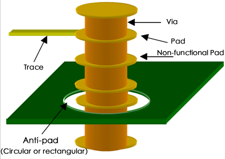
"Through-holes on printed circuit boards (PCBs) are significant points of impedance discontinuity, and optimizing the hole, pad, and anti-pad diameters can significantly improve the impedance continuity issue.
The pad, which supports the hole, can be minimized as much as possible while ensuring welding reliability and manufacturing cost efficiency, by referring to the actual process parameters of PCB pads, to reduce impedance discontinuity at this location.
For high-speed applications, non-functional pads (except for top and bottom layers) should be removed, as shown in the figure below.
For high-speed applications, the size of anti-pads should be maximized to the extent that differential trace reference ground continuity is ensured.
To achieve better transmission performance in high-speed applications, it is recommended to use materials such as FR4 N4103-13SI or materials with a dielectric loss factor of less than 0.008 for the PCB substrate."
Drill hole, finished hole, pad and anti-pad hole size
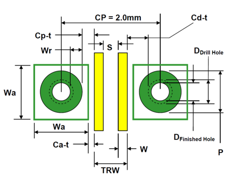
Sub-board mm | Backplane mm | ||
Column Pitch | CP | 2 | 2 |
Drill Hole | Ddrill Hole | 0.7 | 0.66 |
Finished Hole | Dfinished Hole | 0.6 | 0.56 |
Line Width | W | 0.15 | 0.15 |
Trace Spacing | S | 0.127 | 0.127 |
Pad | P | 1.0 | 0.96 |
Anti-pad | Wa | 1.5 | 1.5 |
Total Bus Width | TRW | 0.427 | 0.427 |
Loop Width | Wr | 0.2 | 0.2 |
Drill Hole to Trace Clearance | Cd-t | 0.4365 | 0.4565 |
Pad to Trace Clearance | Cp-t | 0.2865 | 0.3065 |
Anti-pad to Trace Clearance | Ca-t | 0.0365 | 0.0365 |
Note: Line Width and Trace Spacing are used as examples only.
Our factory

The Evolution and ···
 and combiner unit (OMU)")
Wavelength Divisio···

Detailed Explanati···

The Working Princi···
Hot Tags:
R&D laboratory
Gigac has introduced numerous precision testing equipment, such as Ixia XGS12, Ixia WaveTest 93, Anritsu, Fujikura, Fluke, JDSU, Agilent, EXFO, DATA-PIXEL, etc., for product development testing and validation.At present, there are over 100 professional engineers, of which 50% are senior engineers. Through standardized testing processes and in line with international professional testing standards, we provide testing in various aspects such as product appearance, performance, compatibility, and solution scenarios to meet the diverse testing needs of global customers.
Numerous research and development achievements
Gigac adopts a research and development model that combines independent research and joint development, and has achieved outstanding results in industrial design and product software and hardware research and development.As data centers continue to expand and grow, a well planned cabling infrastructure is crucial. Without flexible cabling plans that can easily adapt to common moves, additions, and changes, your network growth will be limited. The Gigac series high-density data center cabling solutions can simplify deployment, enabling up to 144 LC fibers in 1U, and enabling flexible expansion and rapid upgrades with increasing business traffic demands.
Gigac Test Center
Gain a comprehensive understanding of Gigac's optical modules, fiber optic jumpers, and enterprise network testing center. We have a comprehensive testing plan, professional testing equipment, and standard testing procedures. We regularly test optical modules, cables, switches, and other products to ensure that we provide high-quality products to our partners.
